In the first part, we talked about four PCB marks: stamp holes, a specific type of holes, solder thief pad and fiducial marks. Today, we’re going to take a look at another four common marks. So let’s get started.

Spark Gap
It’s for ESD, current surges and over voltage protection. The high voltage will ionize the air between the two terminals and a spark will form across them before it damages the rest of the circuit. It’s not advised to use this way of protection, but it’s better than nothing.
According to an issue published by Microchip, the main drawback is that performance can change over time. The breakdown voltage can be calculated with the following formula V=((3000×p×d)+1350), where “p” is the pressure in atmospheres and “d” is the distance in millimetres.
For more information about spark gaps, you definitely need to watch Dave’s 20-min-long video about spark gaps (it includes real experiments).
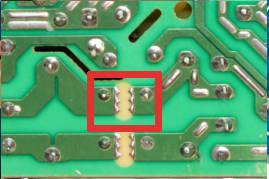
PCB Conductive Button

If you have ever torn down a remote control or a calculator,
Fuse Trace

Similar to the Spark Gap, this is another cheap technique using PCB. The fuse trace is a necked trace on the power line, and it’s a one-shot fuse. The same configuration can be used as a PCB jumper to remove a certain connection by simply etching the necked trace (the PCB jumper can be found in some Arduino UNO boards on the Reset line). To know more about the downsides of using a fuse trace, read this related question on StackExchange.
Slots

If you look into a high voltage device PCB like power supply, probably you will notice some air slots between some traces.
Repeated temporary electrical arcs in a PCB causes the carbonation of the PCB, which leads to a short circuit. To this end, a routed slots can be added in suspected areas, where arcs can still occur but nothing will be carbonized.
Is there any other mark, you have seen, and never know why it’s there? Mention it in a comment please .