If you’re an electronics hobbyist and you hold a new PCB with your bare hands, usually you will spend several minuets staring at it. You want to capture all the art behind it and to see if there is any new technique should be adapted in your next PCB design, but sometimes you can find some marks, and can’t figure out their functionality. In this micro blog I will introduce 4 common PCB marks like these.
Four Common PCB Marks:

Stamp Holes
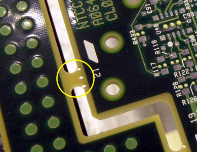
When PCBs are manufactured, they aren’t printed one by one. A number of PCB copies are gathered inside a panel; as many as the panel can fit. This action is called panelization. Now, to make de-panelization easy, cuts are made between the copies and a small contact areas are kept in the fiber. This areas have holes in them which are called stamp holes. I think it’s called a stamp because it will leave an edge like the edge of a stamp when the boards are separated. [UPDATE] This mark has another name: mouse bites. Thanks to darryln for sharing this information.
Types of Holes

In many cases you may see mounting holes surrounded by tiny VIAs. After some search, I found an answer on StackExchange explains this. We have 2 type of mounting holes: plated and un-plated. The surrounding VIAs may be used for 2 reasons:
- When we want to connect the hole with an inner layer (like GND in multi-layer PCBs).
- In case of un-plated hole; When we want to connect the upper pad with the bottom one.

Solder Thief Pad
One of the defects in wave soldering is the soldering bridges especially for SMD parts, and as a solution, it was found that using an extra pad in the end of the pins raw will solve the problem. The width of the extra pad is 2-3 times of the regular one.
It’s called robber pad (AKA solder-thieving) because it take the excess of the solder and prevents any soldering bridges.
Fiducial Marks

A bare copper circle inside a bigger a bare circle. This fiducial mark is used as a reference point for Pick and Place (PnP) machines. Fiducial marks are placed in three places:
- In the panel.
- Beside parts with small pitches like QFN,TQFP .. etc.
- In the PCB corners.

Is there any other mark, you have seen, and never know why it’s there? Mention it in a comment please .
Know more marks in the second part.